

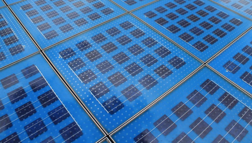
Solar (or photovoltaic) cells harness energy from the sun and convert it into electric current. Until 2008, these devices had a global generation capacity of around just 10 gigawatts (GW), but this figure now stands at roughly 600 GW, which is enough to power a country as big as Brazil. What is more, the power generated by solar cells is estimated to have increased by 22% in 2019 to 720 TWh (terawatt hours), which means that this technology now accounts for almost 3% of worldwide electricity productionLes cellules solaires (ou photovoltaïques) captent l’énergie du soleil et la convertissent en énergie électrique. Jusqu’en 2008, la capacité de production était d’environ 10 gigawatts (GW) au niveau mondial, mais elle est désormais supérieure à 600 GW – ce qui serait suffisant pour alimenter un pays grand comme le Brésil. De plus, la puissance générée par les cellules solaires aurait augmenté de 22 % en 2019 pour atteindre 720 TWh (terawatt hours), ce qui signifie que cette technologie représente désormais près de 3 % de la production mondiale d’électricité1.
These figures will continue to increase as energy production becomes more sustainable and because demand is increasing worldwide. It is up to us, researchers and R&D and technology players, to meet this demand with new designs, efficient photovoltaic materials and new manufacturing processes.
Rapid growth
Such rapid growth is all the more astonishing in that it has happened without any real fundamental change to the underlying photovoltaic technology. Indeed, today’s solar cells are to all intents and purposes similar to the one demonstrated at Bell Laboratories in the US in 1954. This solar cell was based on a simple junction between n‑type (electron-rich) and p‑type (electron-poor) silicon and it converted sunlight into electricity with an efficiency of 5%.
Over the years, this efficiency has gradually increased to over 25% thanks to more advanced cell designs containing highly doped silicon, improved electrical contacts and anti-reflection layers, Silicon-based devices are now cheaper too: the average module price is about $0.21/Wp and the LCOE (levelised cost of energy) is 2.8–6.8 cents/kWh (AC). According to the ITRPV 2020 Report2, these figures will improve, with an expected LCOE in 2031 of 2–5 cents/kWh. These impressive advances, and the fact that the cells can operate for more than 25 years, are the reasons why this technology now accounts for about 95% of the global solar market. New materials could further increase this market share.
The search is on for alternative materials
For PVs to be used in applications such as BI-PV (Building-Integrated PV) or to meet the growing demand for production capacity, silicon (Si) alone no longer fits the bill. That said, Si technology is so efficient and inexpensive that improving it further is difficult. One strategy for overtaking Si is to develop PVs with even higher power conversion efficiencies, i.e. those that convert a larger fraction of sunlight into electricity.
To achieve this, researchers are looking for alternative materials. Thin films based on compounds such as cadmium telluride (CdTe) and copper indium gallium (CuInGa) arsenide, for example, are already commercially available. These materials only need to be a few microns thick to sufficiently absorb solar radiation. They can get away with having a lower quality too (unlike traditional Si). Panels made from these materials can even be flexible.
There is a problem, however, in that these photovoltaic materials rely on indium and tellurium, elements that are rare and thus expensive.
Perovskites, tandem and multi-junction solar cells
In the hunt for more Earth-abundant absorber materials, researchers have turned their attention in recent years to perovskites, promising crystalline materials for thin-film solar cells that can absorb light over a wide range of wavelengths in the solar spectrum. Even though their stability needs to be improved, their efficiency is now above 18%, putting them on a par with established solar cell materials.
Another possibility: ‘tandem’ devices, which are solar cells containing two different but complementary photoactive semiconductor materials. These cells can achieve higher efficiencies when the two materials are used together, compared to either material on its own (the theoretical maximum conversion efficiency increases from 33 to 45%). Combining Si with a perovskite3, for example, can make the most of the different wavelengths of sunlight: silicon efficiently converts photons in the infrared range and perovskites convert higher energy photons.
Further improvements are possible by stacking several photoactive semiconductor materials and carefully choosing the combination that best captures solar radiation. These multi-material devices are called ‘multi-junction cells4 and are mainly based on so-called III‑V materials (GaAs type).
It is not easy to manufacture such devices, however. A solar cell, whatever its architecture, contains different layers of material. Each layer has a crucial role to play: in addition to the photoactive material that absorbs light, we need layers that collect electrons, layers that are transparent to photons, and coatings resistant to humidity, etc. To make an efficient solar cell, each layer must meet strict specifications and be assembled with extreme precision.
Atomic layer deposition
This is where our expertise lies. We synthesise thin films of materials for photovoltaic cells using a technique widely used in the microelectronics industry called Atomic Layer Deposition (ALD)5. Here, the surface of a substrate is successively exposed to a compound, called a precursor, which reacts with the substrate, attaches to it and forms an atomic monolayer. Material growth continues by exposing this layer to a complementary molecule to build the entire structure monolayer by monolayer. This technique allows us to make layers as thin as 2 to 100 nanometres.
Not all molecules are suitable for ALD though. In our laboratory we are trying to understand which molecules are best suited to the technique and which are not, how they behave on the surface of a substrate and what physical and electronic properties they bring to the end material.
Although we are now spoilt for choice for when it comes to the different photovoltaic materials available and under development, it is difficult to predict which ones will win the race. It is possible that several similar complementary technologies will co-exist, with different materials finding different applications. Silicon, combined with a second photoactive material, may remain the material of choice for rigid panels, while thin films will be best for buildings or objects. Whatever the future holds, we are on the verge of a real ‘materials revolution’ for solar cell technology.